Complex Shapes in KiCad
The board design for the SNES wireless controller project is proceeding nicely. I recently finished the main controller schematic, after running into multiple difficulties about how exactly to implement its electronics. Next up: laying out the circuit board. This presented its own set of challenges, which eventually led to me developing a powerful tool for simplifying the layout of complicated circuit boards.
Capturing the PCB dimensions
Below is a scan I made of the back of the Official Nintendo SNES Controller PCB:
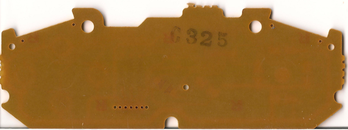
This picture shows the dimensions of the circuit board, without any distracting traces or solder pads. You can clearly see that the shape of this board is relatively complex: It has semicircular cutouts on 3 of its sides. These cutouts wrap around plastic columns on the inside of the SNES Controller. Additionally, the top corners have angled cutouts. These cutouts are designed to leave just enough space for the trigger circuit boards to fit in. The dimensions of the above features are a critical feature of this PCB. If the trigger slots are too deep, the trigger PCB will have room to slide around, possibly impacting the reliability of the trigger buttons. Likewise, if the semicircular cutouts are off by too much, the PCB will not fit in the original controller.
I decided to capture the Controller dimensions in a 2D CAD program, before attempting to design the PCB. This would provide me with a detailed reference I could use when actually designing the dimensions of the real PCB. There are several reasons to use a 2D CAD program instead of directly implementing the board dimensions in EDA software. First of all, the 2D CAD software has much more powerful tools for creating accurate drawings. Secondly, it is useful to have the footprint in a format that would make it easy to test mechanical prototypes: The output from the 2D CAD program can be passed to a laser cutter. This will create a test board useful for verifying the dimensions of replacement PCB.
I decided to use the open source CAD program QCAD. This program made it relatively easy to capture the PCB dimensions.
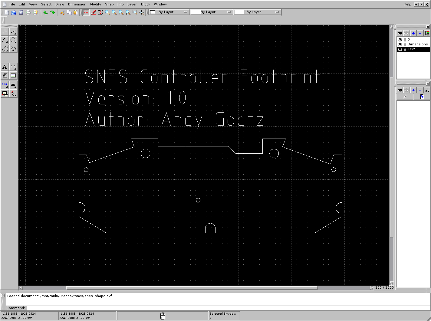
I started by using GIMP to measure the dimensions of the circuit board from the high-resolution scan shown above. This let me get a rough estimate of the dimensions of the PCB. I then printed out a copy of the design, and tried to align the PCB with the CAD drawing. Any misalignments were adjusted in QCAD, until a footprint was created that matched the SNES Controller perfectly.
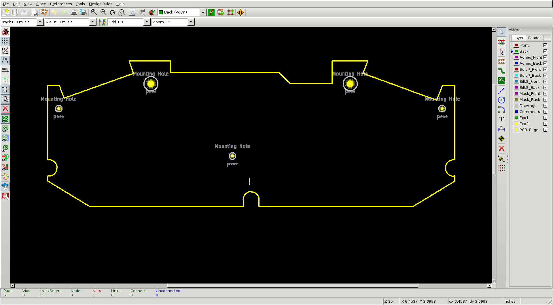
My original plan called for drawing the PCB footprint in KiCad at this time. It was at this point that I ran into another major problem. Take a look at these example kicad screenshots.
You should immediately notice that all of these PCBs are rectangular. The edges are all much simpler than the SNES PCB. There is a very good reason for this: The drawing tools in KiCad stink. You can only create lines, circles, rectangles and arcs, and these elements must be placed essentially freehand. There is no way to manually enter the dimensions or angle of any of these elements. In addition, the arc tool only allows for 90 degree curves.
I had just spent several painstaking hours importing the SNES dimensions into QCAD. I did not want to throw away all of this work just to start over again in KiCad. In addition, I did not want to maintain two separate copies of the SNES footprint, one in QCAD and one in KiCad.
That is when it struck me. What if I wrote a converter to convert the QCAD files into a format that KiCad could understand?
Introducing dxf2brd
QCAD stores its drawing in a file format called DXF. DXF stands for Drawing Interchange Format. This is an old file format created by Autodesk, and it serves as a lingua franca in the world of Mechanical Manufacturing. Crucially, there exist several open source libraries to parse DXF files.
Kicad stores PCB design data in a custom file format called BRD. This file format is simple ascii, and is fairly easy to parse.
dxf2brd is a simple helper utility that reads DXF files, and translates lines, circles and arcs from the DXF file to the Kicad BRD coordinate space. In addition, it converts circles in the DXF file into mechanical holes that Kicad can use to create the drill file.
Conclusion
Overall, I am extremely happy with the combination of QCAD and KiCad. Using QCAD to draw complex shapes is much easier than trying force the design in Kicad, and it allows us to use standard rapid prototyping tools, such as a laser-cutter, to make sure the dimensions match perfectly. Additionally, the dxf2brd tool makes it a snap to design complex circuit boards in a real CAD tool, before exporting the results into EDA tools.
Source Files: dxf2brd snes_shape.dxf scanner.brd